- 您现在的位置:买卖IC网 > Sheet目录489 > NTJD1155LT1 (ON Semiconductor)MOSFET/LOAD SWITCH HI 8V SOT-363
NTJD1155L
Power MOSFET
8 V, + 1.3 A, High Side Load Switch with
Level ? Shift, P ? Channel SC ? 88
The NTJD1155L integrates a P and N ? Channel MOSFET in a single
package. This device is particularly suited for portable electronic
equipment where low control signals, low battery voltages and high
http://onsemi.com
load currents are needed. The P ? Channel device is specifically
designed as a load switch using ON Semiconductor state ? of ? the ? art
trench technology. The N ? Channel, with an external resistor (R1),
functions as a level ? shift to drive the P ? Channel. The N ? Channel
MOSFET has internal ESD protection and can be driven by logic
signals as low as 1.5 V. The NTJD1155L operates on supply lines from
V (BR)DSS
8.0 V
R DS(on) TYP
130 m W @ ? 4.5 V
170 m W @ ? 2.5 V
260 m W @ ? 1.8 V
I D MAX
± 1.3 A
1.8 to 8.0 V and can drive loads up to 1.3 A with 8.0 V applied to both
V IN and V ON/OFF.
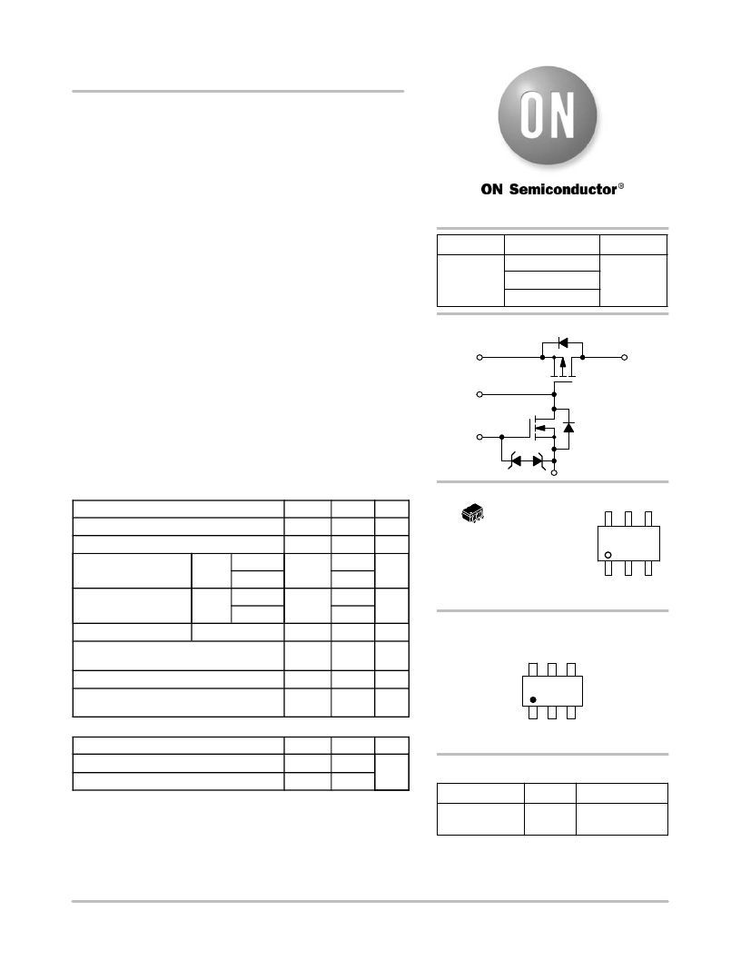
SIMPLIFIED SCHEMATIC
Features
? Extremely Low R DS(on) P ? Channel Load Switch MOSFET
? Level Shift MOSFET is ESD Protected
? Low Profile, Small Footprint Package
? V IN Range 1.8 to 8.0 V
? ON/OFF Range 1.5 to 8.0 V
? These Devices are Pb ? Free and are RoHS Compliant
4
6
5
1
Q2
Q1
2,3
T A = 85 ° C
T A = 85 ° C
1
MAXIMUM RATINGS (T J = 25 ° C unless otherwise noted)
Rating Symbol
Input Voltage (V DSS , P ? Ch) V IN
ON/OFF Voltage (V GS , N ? Ch) V ON/OFF
Continuous Load Current Steady T A = 25 ° C I L
(Note 1) State
Power Dissipation Steady T A = 25 ° C P D
(Note 1) State
Pulsed Load Current t p = 10 m s I LM
Value
8.0
8.0
± 1.3
± 0.9
0.40
0.20
± 3.9
Unit
V
V
A
W
A
MARKING
SC ? 88 DIAGRAM
(SOT ? 363)
CASE 419B
STYLE 30 TB M G
G
TB = Device Code
M = Date Code 1
G = Pb ? Free Package
(Note: Microdot may be in either location)
PIN ASSIGNMENT
Operating Junction and Storage Temperature
T J ,
T STG
? 55 to
150
° C
D1/G2
6
G1
5
S2
4
Source Current (Body Diode)
Lead Temperature for Soldering Purposes
(1/8 ″ from case for 10 s)
I S
T L
? 0.4
260
A
° C
THERMAL CHARACTERISTICS
Characteristic
Symbol
Max
Unit
1
S1
2 3
D2 D2
Junction ? to ? Ambient – Steady State (Note 1) R q JA 320 ° C/W
Junction ? to ? Foot – Steady State (Note 1) R q JF 220
Stresses exceeding Maximum Ratings may damage the device. Maximum
Ratings are stress ratings only. Functional operation above the Recommended
Operating Conditions is not implied. Extended exposure to stresses above the
Recommended Operating Conditions may affect device reliability.
1. Surface ? mounted on FR4 board using 1 inch sq pad size
(Cu area = 1.127 in sq [1 oz] including traces).
ORDERING INFORMATION
Device Package Shipping ?
NTJD1155LT1G SC ? 88 3000/Tape & Reel
(Pb ? Free)
?For information on tape and reel specifications,
including part orientation and tape sizes, please
refer to our Tape and Reel Packaging Specification
Brochure, BRD8011/D.
? Semiconductor Components Industries, LLC, 2012
November, 2012 ? Rev. 5
1
Publication Order Number:
NTJD1155L/D
发布紧急采购,3分钟左右您将得到回复。
相关PDF资料
NTJD2152PT4G
MOSFET P-CH 8V DUAL ESD SOT-363
NTJD4001NT2G
MOSFET N-CH DUAL 30V SOT-363
NTJD4105CT2G
MOSFET N/P-CHAN COMPL SOT-363
NTJD4152PT1
MOSFET P-CHAN DUAL 20V SOT-363
NTJD4158CT1G
MOSFET N/P-CHAN COMPL SOT-363
NTJD4401NT1G
MOSFET 2N-CH 20V 630MA SOT-363
NTJD5121NT2G
MOSFET N-CH 60V DUAL ESD SOT363
NTJS3151PT1G
MOSFET P-CH 12V 2.7A SOT-363
相关代理商/技术参数
NTJD1155LT1G
功能描述:MOSFET 8V +/-1.3A P-Channel w/Level Shift RoHS:否 制造商:STMicroelectronics 晶体管极性:N-Channel 汲极/源极击穿电压:650 V 闸/源击穿电压:25 V 漏极连续电流:130 A 电阻汲极/源极 RDS(导通):0.014 Ohms 配置:Single 最大工作温度: 安装风格:Through Hole 封装 / 箱体:Max247 封装:Tube
NTJD116N
制造商:ONSEMI 制造商全称:ON Semiconductor 功能描述:High Efficiency DC-DC Converters
NTJD2152P
制造商:ONSEMI 制造商全称:ON Semiconductor 功能描述:Trench Small Signal MOSFET
NTJD2152P_06
制造商:ONSEMI 制造商全称:ON Semiconductor 功能描述:Trench Small Signal MOSFET
NTJD2152PT1
功能描述:MOSFET 8V Dual P-Channel RoHS:否 制造商:STMicroelectronics 晶体管极性:N-Channel 汲极/源极击穿电压:650 V 闸/源击穿电压:25 V 漏极连续电流:130 A 电阻汲极/源极 RDS(导通):0.014 Ohms 配置:Single 最大工作温度: 安装风格:Through Hole 封装 / 箱体:Max247 封装:Tube
NTJD2152PT1G
功能描述:MOSFET 8V Dual P-Channel ESD Protection RoHS:否 制造商:STMicroelectronics 晶体管极性:N-Channel 汲极/源极击穿电压:650 V 闸/源击穿电压:25 V 漏极连续电流:130 A 电阻汲极/源极 RDS(导通):0.014 Ohms 配置:Single 最大工作温度: 安装风格:Through Hole 封装 / 箱体:Max247 封装:Tube
NTJD2152PT2
功能描述:MOSFET 8V Dual P-Channel RoHS:否 制造商:STMicroelectronics 晶体管极性:N-Channel 汲极/源极击穿电压:650 V 闸/源击穿电压:25 V 漏极连续电流:130 A 电阻汲极/源极 RDS(导通):0.014 Ohms 配置:Single 最大工作温度: 安装风格:Through Hole 封装 / 箱体:Max247 封装:Tube
NTJD2152PT2G
功能描述:MOSFET 8V Dual P-Channel ESD Protection RoHS:否 制造商:STMicroelectronics 晶体管极性:N-Channel 汲极/源极击穿电压:650 V 闸/源击穿电压:25 V 漏极连续电流:130 A 电阻汲极/源极 RDS(导通):0.014 Ohms 配置:Single 最大工作温度: 安装风格:Through Hole 封装 / 箱体:Max247 封装:Tube
